1.2 KiB
VLSI Homework 12 - Aidan Sharpe
Problem 12.5
Estimate the minimum delay of a 10:1024 decoder driving an electrical effort of H=20.
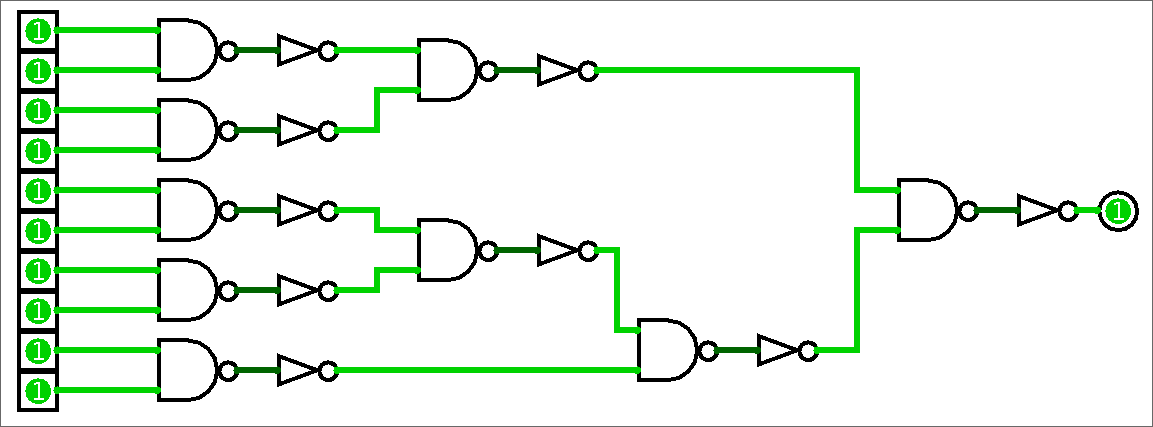
A 10:1024 decoder will contain 1024 AND gates. It will have a branching effort of B=1024/2=512. Assuming G\approx1 for a 10-input AND gate, the path effort will be F=GBH=40960. The optimal number of stages will be, assuming the stage effort is \rho=4, \hat{N} = \log_4(40960)=7.66. We will use 8 stages in our solution, seen below.
Using static CMOS gates
For a static CMOS design, G = (4/3)^4 = 256/81. Therefore, the actual stage effort is F = GBH = 32363.5. The parasitic delay is P = 12, so the total delay will be D=NF^{1/N} + P = 41.3\tau.
Using footless domino gates
A footless domino design has g=1/3 for inverters and g=2/3 for NAND2. Therefore, G=(1/3)^4(2/3)^4=16/6561, and F=GBH=24.97. The parasitic delay for inverters is p=2/3, and p=1 for NAND2. Therefore, the path parasitic delay is P=4 + 8/3 = 20/3. Finally, the total delay will be D=NF^{1/n} + P = 18.62\tau.
Problem 12.12
NAND ROMs will have a higher resistance than a comparable NOR ROM, thereby making them slower.
